The rise of artificial intelligence is reshaping the global semiconductor industry. As demand for large language models, generative AI, and high-performance computing accelerates, the volume of data that compute chips must handle is growing exponentially. In this environment, traditional memory technologies are hitting bandwidth and power efficiency limits, while HBM (High Bandwidth Memory)—which enables ultra-fast data transfer—has become a cornerstone of AI infrastructure.
In the global HBM market, SK Hynix holds a significant position. As one of the world's leading memory chip manufacturers, SK Hynix has not only deep expertise in DRAM but also took an early lead in HBM product development and mass production. With AI GPUs demanding ever-faster memory, SK Hynix has emerged as a key supplier in the AI memory chip supply chain.
What Is HBM?
HBM (High Bandwidth Memory) is a high-bandwidth memory technology purpose-built for AI, high-performance computing (HPC), data centers, and graphics processing. Compared to traditional DRAM, HBM delivers far greater data throughput in a much smaller space.
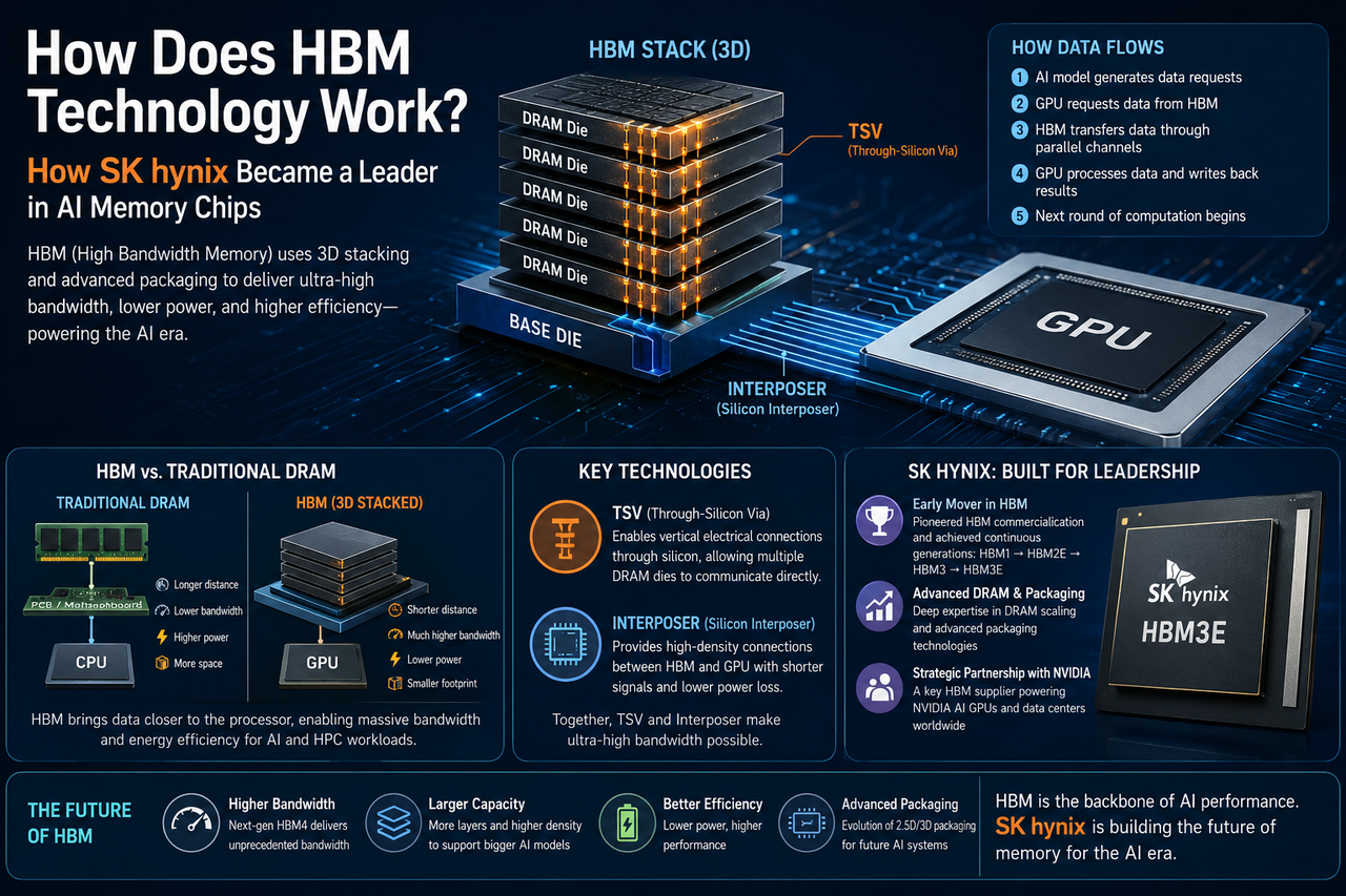
The key innovation of HBM is its 3D stacking architecture, where multiple DRAM chips are stacked vertically and interconnected at high speeds using TSV (Through-Silicon Via) technology. Because data travels shorter distances, HBM dramatically boosts bandwidth while cutting power consumption.
Why Traditional DRAM Falls Short for AI
For years, traditional DRAM has been the go-to memory solution for computers and servers. But the data demands of the AI era have far outstripped those of conventional computing.
During large model training, GPUs must constantly read and write enormous numbers of parameters. If data can't move fast enough to keep the GPU fed, even the most powerful processors waste cycles waiting.
Traditional DRAM struggles with:
| Challenge |
Traditional DRAM Performance |
| Bandwidth ceiling |
Limited data throughput |
| High power draw |
Longer data paths increase energy use |
| Large physical footprint |
Hard to fit in dense deployments |
| AI scalability |
Efficiency drops in multi-GPU setups |
That's why the industry has turned to new memory architectures better suited to AI—and HBM has taken off.
How HBM Technology Works
HBM's core idea: shorten the distance data must travel and significantly increase the number of data channels.
Traditional DRAM connects to the processor through the motherboard. HBM, by contrast, is packaged directly alongside the GPU. Multiple DRAM dies are stacked vertically using TSV, and a silicon interposer links them to the GPU for ultra-high-bandwidth communication.
The data flow works like this:
- An AI model running on the GPU generates a constant stream of data requests.
- The GPU sends read commands to HBM.
- HBM feeds data back through multiple parallel channels at blazing speed.
- Once computation finishes, the GPU writes results back to memory.
- The next cycle of computation begins immediately.
This design minimizes latency from data movement and dramatically improves AI training efficiency.
HBM vs. Traditional DRAM: Structural Differences
| Dimension |
HBM |
Traditional DRAM |
| Chip architecture |
3D stacked |
Planar layout |
| Data interconnect |
TSV + Interposer |
PCB traces |
| Bandwidth |
Ultra-high |
Moderate |
| Power consumption |
Lower |
Higher |
| Primary use cases |
AI, GPU, HPC |
PCs, servers |
Why TSV and Interposer Matter
TSV (Through-Silicon Via) is the enabling technology for HBM's 3D stacking. It creates vertical channels through the chip, allowing stacked memory layers to communicate directly with one another. The interposer (silicon interposer) serves as the connection bridge between the GPU and HBM, providing far denser data pathways and lower signal loss than traditional motherboard traces.
Together, these two technologies form the backbone of HBM's architecture and are the primary reasons it can achieve such extreme bandwidth.
HBM's Role in AI Training
Modern AI models contain billions or even trillions of parameters. Each training run requires reading vast datasets.
If the GPU computes faster than data can be supplied, the system experiences computing power idling. HBM's job is to keep the data pipeline full, ensuring the GPU can work at peak efficiency.
In AI inference, HBM is equally critical. Fast memory access speeds up response times and improves model performance. That's why HBM has become an indispensable part of AI chip design.
How SK Hynix Became the HBM Leader
SK Hynix has deep roots in DRAM technology, which laid the groundwork for its HBM breakthroughs.
The company was among the first to commercialize HBM. From HBM1 to HBM3E, SK Hynix has steadily pushed the envelope on bandwidth, capacity, energy efficiency, and advanced packaging.
Before the AI frenzy, the HBM market was relatively niche. Yet SK Hynix kept investing in R&D. By the time generative AI and large models sent demand through the roof, the company already had mature technology and production capacity ready to go.
This long-term strategic positioning gave SK Hynix a formidable competitive edge.
SK Hynix and NVIDIA: A Strategic Partnership
AI GPUs are the largest application market for HBM, and NVIDIA is a major player in the AI chip space.
Today's top-tier AI GPUs require massive, high-bandwidth memory subsystems. HBM has become the standard for high-end GPUs, and SK Hynix is a key HBM supplier.
This relationship lets SK Hynix play a central role in building AI infrastructure—and strengthens its strategic importance in the global semiconductor supply chain.
The Future of HBM
As AI models keep growing, HBM technology continues to evolve.
Key trends on the horizon:
| Technology Direction |
Goal |
| HBM4 |
Even higher bandwidth and capacity |
| More stacking layers |
Greater memory density |
| Advanced packaging |
Lower latency and power |
| AI-optimized memory |
Better training efficiency |
| Chiplet integration |
Improved system scalability |
Going forward, performance gains in AI chips will depend not just on the GPU itself, but increasingly on memory innovation.
HBM vs. GDDR: What's the Difference?
Both HBM and GDDR are high-performance memories, but they're designed for different jobs.
GDDR is built for consumer graphics cards, boosting speed through higher clock frequencies. HBM, by contrast, achieves its performance through an ultra-wide bus and vertical stacking, offering higher bandwidth and lower power. In AI training, HPC, and data center environments, HBM typically has the clear advantage.
Summary
HBM is one of the most important memory technologies of the AI era. Through 3D stacking, TSV, and silicon interposers, it delivers bandwidth that far surpasses traditional DRAM. As large model training and high-performance computing demand more, HBM has become essential to AI GPUs and data center infrastructure.
Thanks to decades of DRAM expertise, advanced packaging skills, and relentless investment in HBM, SK Hynix has established itself as a global leader. From AI chips to data centers, GPUs to supercomputers, HBM is powering the growth of AI compute—and SK Hynix sits at the center of this critical supply chain.
FAQs
Why is HBM better for AI than traditional DRAM?
HBM provides much higher bandwidth, lower latency, and lower power consumption. AI model training constantly reads huge datasets, so HBM is a far better match for GPU memory needs.
What is TSV technology?
TSV (Through-Silicon Via) creates vertical electrical connections through stacked chips. HBM uses TSV to achieve dense 3D packaging.
What's the difference between HBM and GDDR?
GDDR is designed for graphics rendering; HBM is built for AI, HPC, and data centers. HBM typically offers superior bandwidth and energy efficiency.
Why is SK Hynix leading the HBM market?
SK Hynix invested in HBM early and has deep expertise in DRAM manufacturing and advanced packaging. When AI demand exploded, the company had mature products and production ready to scale.
What will HBM4 change?
HBM4 is expected to push bandwidth, capacity, and energy efficiency even further, supporting larger AI training workloads. As AI compute continues to scale, HBM4 is expected to become an important memory solution for next-generation high-performance platforms.